See here for my review of the M001.
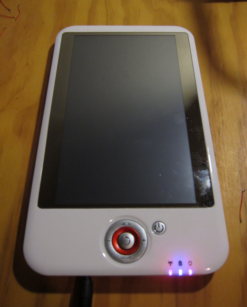
This teardown shows the V006 revision of the board, a quick serial port install, and includes some console/dmesg output. The main difference between V005 and V006/V007 board revisions seems to be relocating the USB WiFi dongle to a better position.
EDIT: It took me a while to post this article, and Slatedroid is down this past week. So links to there will be broken (hopefully not for good.)
This isn't the first teardown of the Eken M001, the first one was the "Aimless Teardown" and there is also a disassembly howto video by another community member.
Warning
I've had lots of hardware problems with my Eken since I took it apart. They may have been there before, but maybe not. YMMV, but be careful and remember you may not still have a warranty after the device has been opened, and especially after it's been modified.
Specifically, I have two problems. There is a cold solder joint in one corner of the board (I'm currently warming it up before it will boot at all.) Also I get occasional failure of the LCD (totally black) on reassembly, which requires me to press on the front of the unit until it clicks back on.
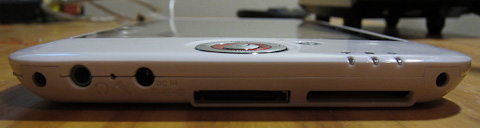
Getting In
-
Remove the two phillips screws on each side of the base:
-
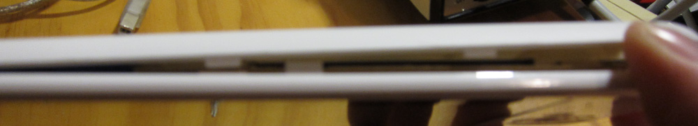
The only other thing holding the back on is a series of plastic clips around the outside of the unit. Working from the base (the first clip is half-way between the two screws), carefully insert a plastic spudger or a knife (worse, but what I used) and jiggle it around until each clip snaps open. Some clips may break, they're not very strong.
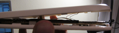
Then work your way along towards the top of the unit:
q
-
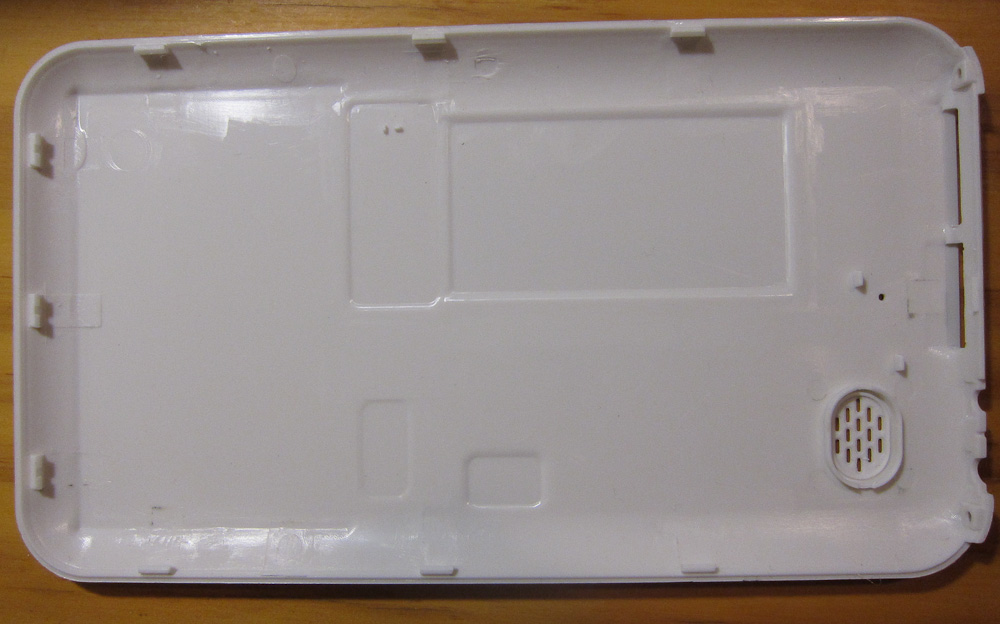
Once all the clips have popped, remove the plastic back. Take care not to disturb the small speaker
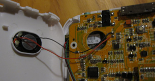
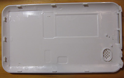
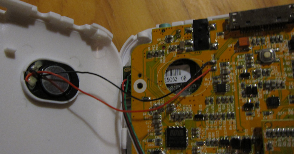
Main Board
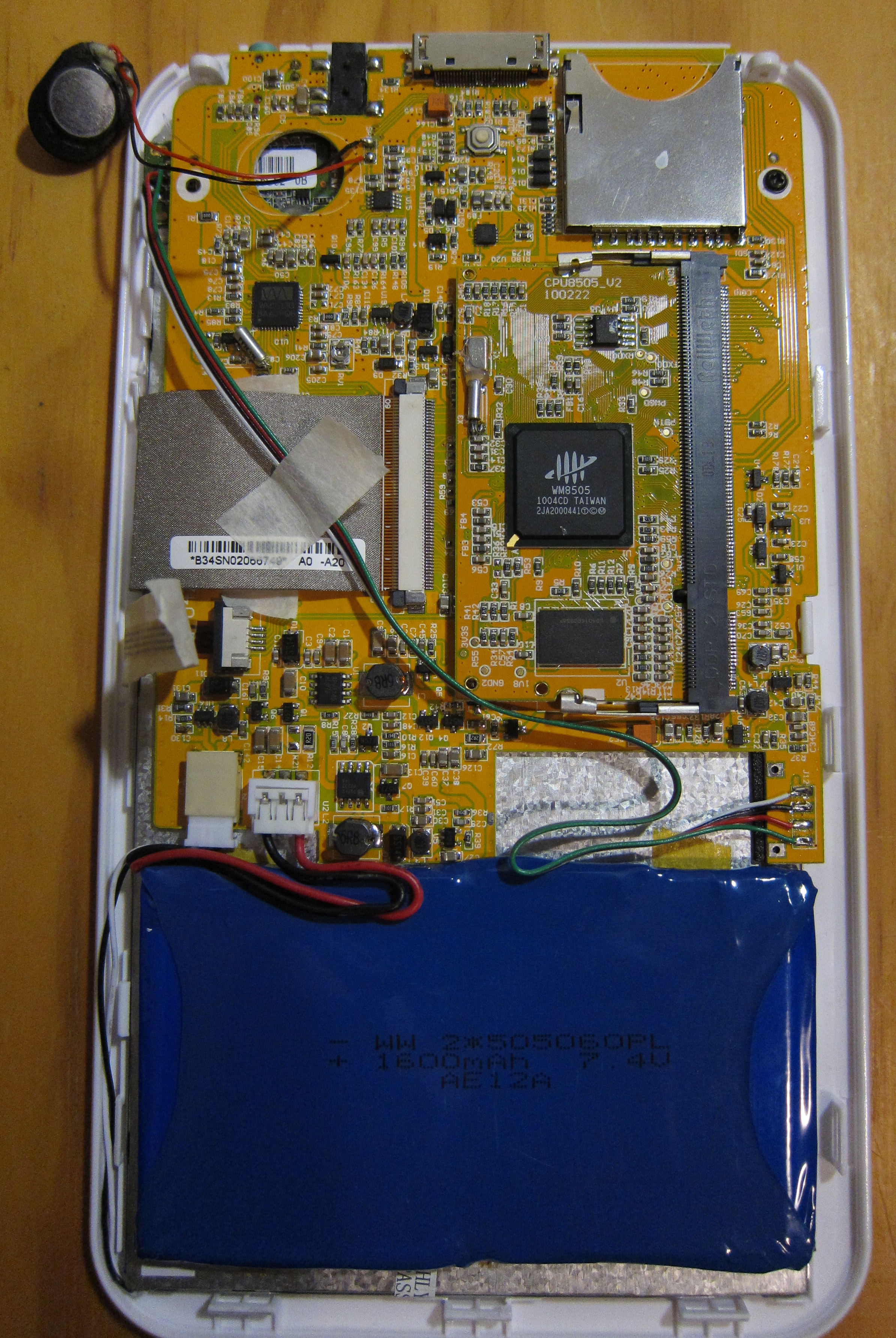
(Click through for a high-res version.)
You can see:
<ul>
<li>
Battery and backlight connectors bottom-leftl
</li>
<li>
Internal USB soldered to pads bottom-right (leading up to the USB WiFi module, installed top left.)
</li>
<li>
LCD and touchscreen ribbon connectors on the left side.
</li>
<li>
Main CPU daughterboard in DIMM socket.
</li>
CPU Board
Here's some shots of the CPU daughterboard:
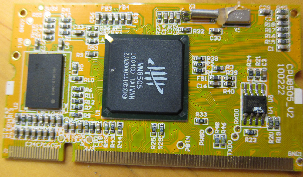
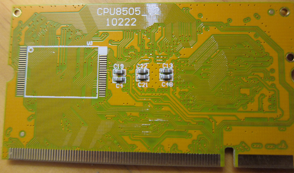
The board is hosting a VIA/Wondermedia WM8505 SoC. Datasheet shared here (courtesy Slatedroid, again.
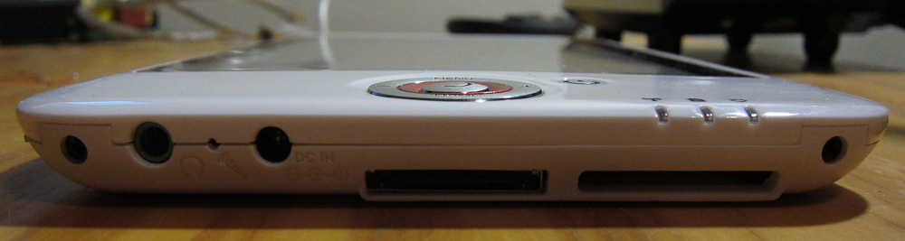
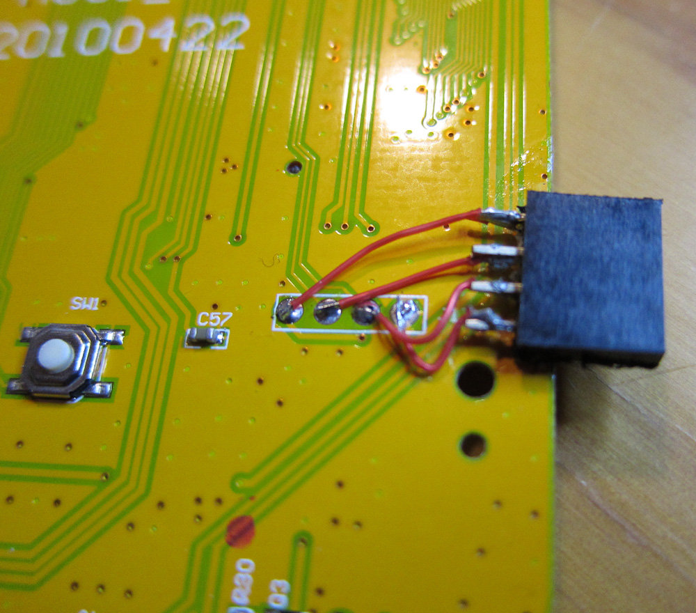
Serial Connector
J17 on the back of the board is a RvTTL (3.3v) serial port. 115200 8N1. Pinout, left to right, is Vcc Tx Rx Gnd.
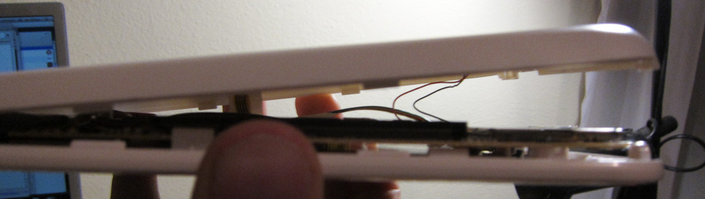
I didn't take any photos of it before I soldered on my serial port, but here it is after:
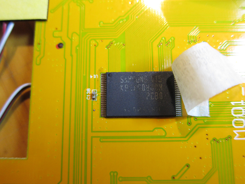
The only other interesting thing I saw on the back of the board was the 2Gb NAND flash:
Boot logs
Once you have the serial port connected, you can grab some log data easily (and you also get a root shell once startup completes.)
EDIT: As of firmware release 1.7.4, no more automatic root shell on serial console. It's still a boot console, but for root you need to log in... Poor show, Eken.
Standard kernel boot log, plus some /proc entries
Log of a factory upgrade via SD card
</p>
I meant to capture and post some of the 'logcat' Android log output as well, from standard startup, but it doesn't look like I kept any.
Thoughts on “Eken M001 teardown & serial console”